Physicists Finally Built a Quantum Material Predicted a Decade Ago. It Conducts Electricity Only Along Its Edges.
For more than a decade, a two-dimensional topological crystalline insulator existed only in equations. Now researchers at the University of Jyväskylä and Aalto University have built one: a two-layer film of tin telluride on niobium diselenide that blocks electricity in its interior while conducting it along its edges. The compressive strain from the substrate stabilizes the topological phase, and the band gap, larger than 0.2 electron volts, should keep the edge states working at room temperature.
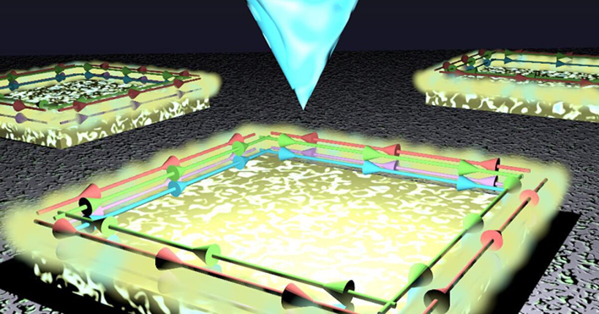
For more than a decade, the material existed only in equations. Physicists had predicted that a sheet of tin telluride just two atomic layers thick could become a topological crystalline insulator, a quantum material that blocks electricity in its interior while letting it flow freely along its edges. But every attempt to build one ran into the same wall. The crystal structure itself kept getting in the way.
In January 2026, a Finnish team finally cleared that wall. Researchers at the University of Jyväskylä, working with colleagues at Aalto University, grew the two-layer film on a carefully chosen substrate and watched electrons travel along its edges in pairs, protected by the symmetry of the crystal. The result, published in Nature Communications, is the first experimental realization of a two-dimensional topological crystalline insulator, a quantum material that theorists sketched out more than ten years ago.
The promise of edge-only conduction
Ordinary materials conduct electricity in one of two ways. Metals let electrons move freely through their bulk. Insulators, like glass or rubber, barely let them move at all. Topological insulators break that binary. Their interiors behave like insulators, but their surfaces or edges conduct, and they do it in a way that ordinary materials cannot imitate.
The conducting edge states are protected by symmetry, the mathematical properties of the crystal that stay the same when the material is transformed in some way. Because the protection comes from the quantum state itself, defects, impurities, and bumps that would scatter electrons in a normal wire cannot easily knock them off course. The electrons keep flowing, which means less wasted energy as heat.
Topological insulators are not new. The first ones were demonstrated in three dimensions more than fifteen years ago, and two-dimensional versions followed. But the two-dimensional topological crystalline insulator, a subtype whose protection comes from the mirror symmetry of the crystal lattice rather than from time-reversal symmetry alone, had stayed out of reach.
Why the two-layer version was so hard
Tin telluride was the obvious candidate. The same compound had already produced three-dimensional topological crystalline insulators, and theory said its ultrathin films should do the same. The catch was in the counting.
Tin telluride crystallizes in the rock-salt structure, the same arrangement as table salt, and each monolayer of the film contains two atomic layers. Theory predicted that only films with an odd number of atomic layers should become topological crystalline insulators, because only those keep the symmetry that protects the edge states. But in the lab, films grow in whole monolayers, which always produces an even number of atomic layers. Every attempt to grow a topological film was stuck with the wrong count.
There was a second problem. In the ultrathin limit, tin telluride develops a strong ferroelectric phase, an electric polarization that shifts the atoms and undoes the band inversion needed for the topological state. Growing the film on a substrate also caused the bottom layer to hybridize with it, muddying the electronic structure.
The strain that flipped the switch
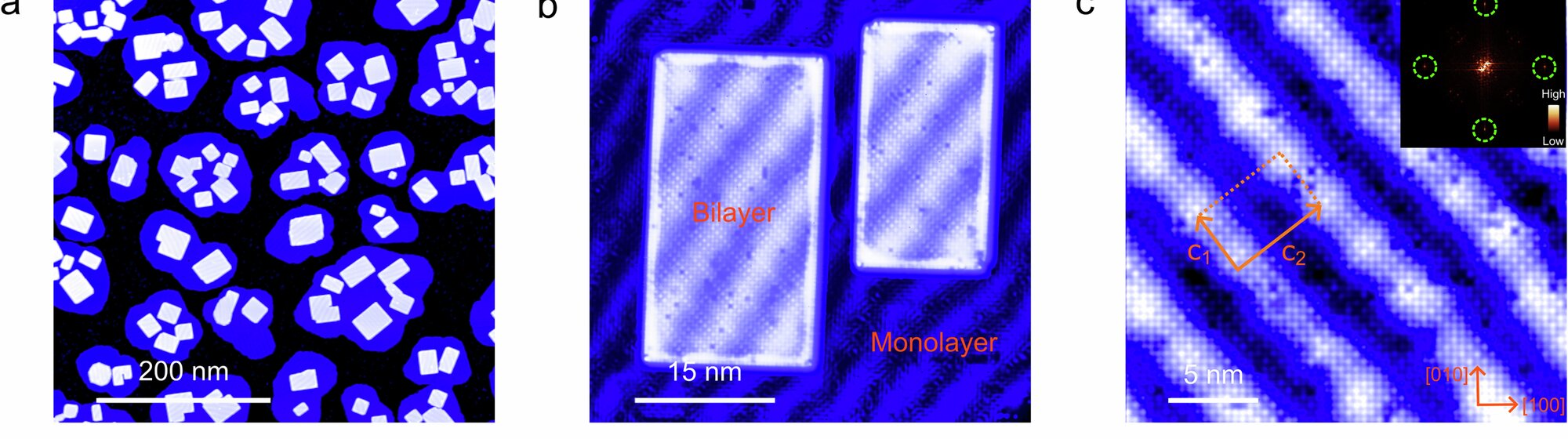
The Finnish team found a way around all three obstacles at once: stop fighting the substrate and use it. They grew bilayer tin telluride on a substrate of niobium diselenide, a metallic compound whose surface lattice does not match tin telluride's. The mismatch squeezes the film, compressing it in both directions, and the strain does the work.
First, the bottom atomic layer bonds tightly to the substrate and becomes decoupled from the three layers above it. That leaves an effective three-layer system, exactly the odd count that theory said was needed. Second, the compressive strain shifts the electronic bands enough to drive the film through a phase transition, from the trivial ferroelectric state that plagued earlier attempts into a topological crystalline insulator.
The strain shows up directly in the microscope images as moiré patterns, the interference stripes that appear when two mismatched lattices overlap. The team measured the compressed lattice constants atom by atom, then fed those numbers into density functional theory calculations, which confirmed that the observed edge states were topological in origin.
Conducting edges with room to spare
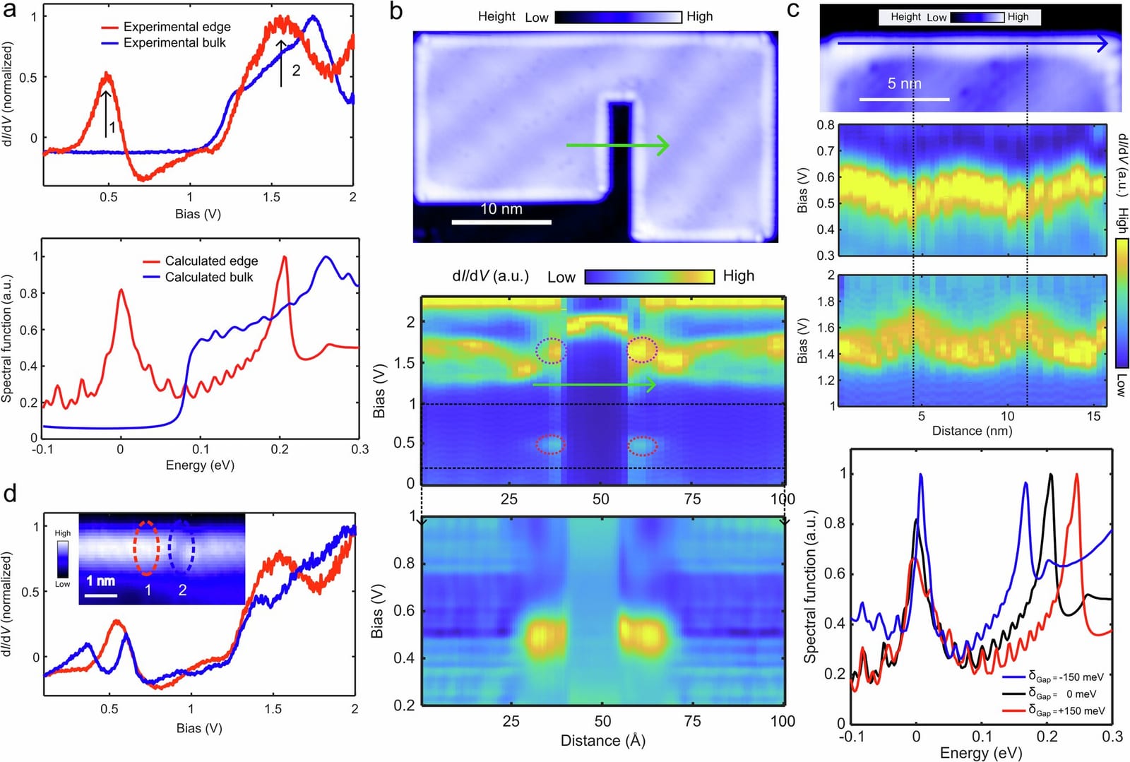
Using low-temperature scanning tunneling microscopy, the researchers mapped the electronic structure of the islands and found pairs of conducting edge states running along their boundaries, the signature of a topological crystalline insulator. The edge states sit inside a band gap of more than 0.2 electron volts, measured directly by the tunneling spectra.
That number matters far beyond the lab. Most previously discovered two-dimensional topological insulators have band gaps of only a few millielectron volts. At room temperature, thermal energy is about 25 millielectron volts, enough to swamp a gap that small and destroy the edge conduction, which is why most topological devices must be cooled to cryogenic temperatures. A gap above 0.2 electron volts is roughly eight times larger than room-temperature thermal energy, so the topological edge states should survive without extreme cooling.
The team also showed the edge states can be tuned. Because the topological phase is stabilized by strain, changing the strain changes the electronic properties, giving engineers a practical knob to turn. And when two islands sit close together, their edge states interact across the gap, shifting energy levels through a combination of electrostatic forces and quantum tunneling, behavior that matters for anyone hoping to wire these materials into circuits.
None of this is a working device yet. The measurements were made at low temperature, and the room-temperature robustness is an expectation based on the size of the band gap, not a demonstration of a room-temperature transistor. But the material now exists, which is the part that was missing for a decade.
What comes next
The obvious applications are in spintronics, electronics that use the spin of the electron as well as its charge, and in nanoscale devices where the edge-only conduction could carry signals with very little energy loss. The strain tunability is the unexpected bonus: a quantum material whose properties can be adjusted after it is grown is far more useful to engineers than one that is fixed at birth.
For physicists, the achievement closes a gap that had been open since the topological crystalline insulator was first predicted. The equations said the material could exist. The substrate, squeezed just right, made it real.
Why this is a different kind of quantum material
Most quantum materials earn the label because of what happens at extremely low temperatures: superconductivity, exotic magnetism, topological order that only appears near absolute zero. This one is interesting for the opposite reason. Its defining feature, the edge conduction, is tied to a band gap large enough that ordinary room-temperature vibrations should not destroy it.
That is what makes the two-dimensional topological crystalline insulator a platform rather than a curiosity. It gives researchers a material where protected, low-loss conduction might work in conditions a real device could tolerate, and it gives them a way to adjust that conduction after the fact. The decade-old prediction has a physical home now.
Sources
- Jing et al., "Strain-induced two-dimensional topological crystalline insulator in bilayer SnTe," Nature Communications 17, 817 (January 21, 2026) - open-access primary research article describing the growth, STM characterization, strain analysis, and density functional theory calculations
- Decade-old theory becomes reality: 2D topological material realized (University of Jyväskylä) - press release from the lead institution with project context and the official illustration
- 2D topological crystalline insulator turns decade-old prediction into reality (Phys.org) - coverage of the research led by Associate Professor Kezilbeiek Shawulienu, with colleagues Peter Liljeroth and Jose Lado at Aalto University
- Physicists finally build a quantum material predicted more than a decade ago (ScienceDaily, July 11, 2026) - summary of the findings with journal reference
Related on Impossible Universe
- Scientists Built LEGO-Like Nanoparticles Into a Material That Shows Quantum Behavior at Room Temperature - another room-temperature quantum material, built from silver nanoparticles that couple to light at ambient conditions
- The First Time Crystal You Can See With Your Own Eyes - an exotic phase of matter that breaks the usual rules of symmetry, also built from carefully engineered materials
- This Tiny Chip Processes Information With Light Instead of Electricity - another path to energy-efficient electronics, processing data with light instead of moving electrons through wires
- Physics and Quantum: The Frontier of How Things Work - more stories from the physics topic hub, from quantum materials to the nature of time
Hero image: University of Jyväskylä / Jose Lado, official press illustration of the system. Inline images: reproduced from Jing et al., Nature Communications 17, 817 (2026), licensed under CC BY 4.0. The research was supported by the European Research Council and the Academy of Finland.