
This Tiny Chip Processes Information With Light Instead of Electricity
Monash University engineers built a nanoscale circuit that uses light instead of electricity to process information. The chip operates at room temperature, handles two data streams at once, and could power a new generation of quantum and optical computing technologies.
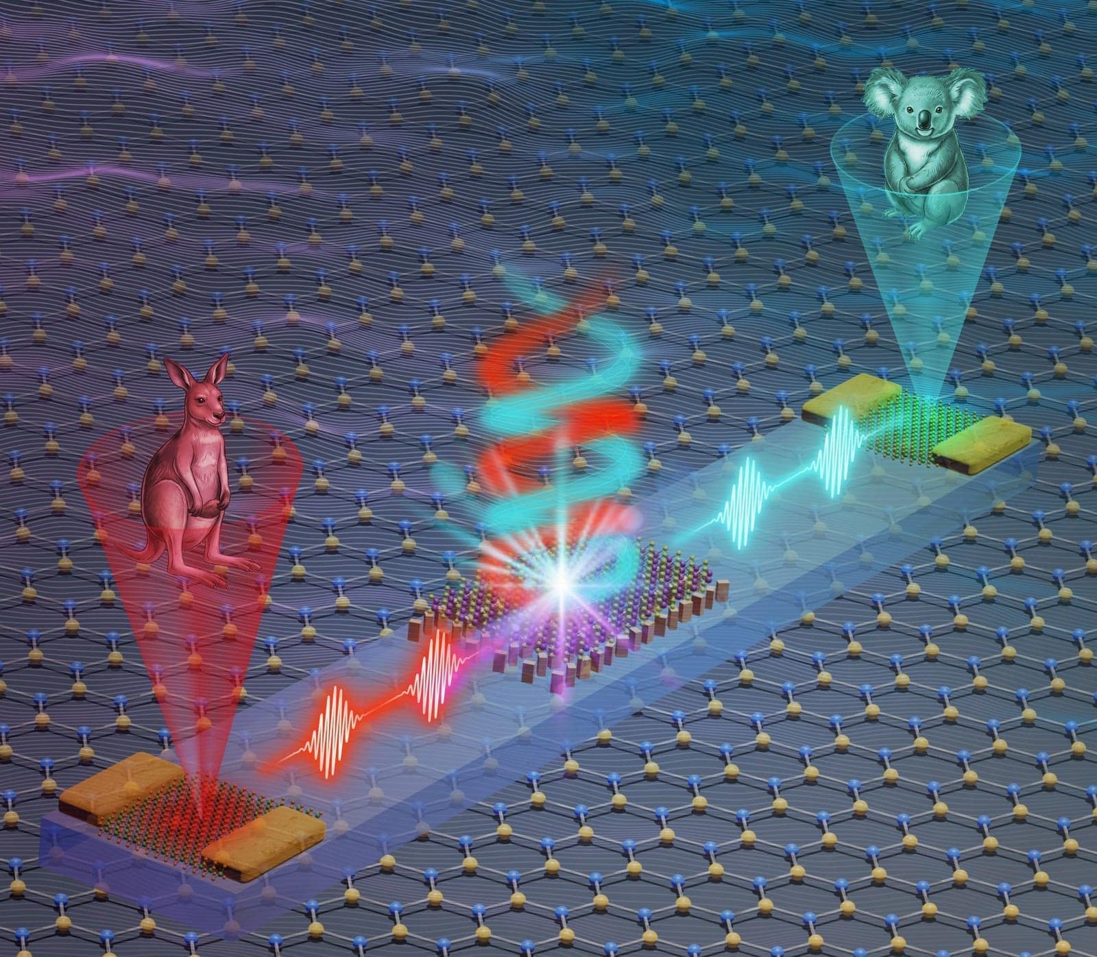
What if a computer could process information using light instead of electricity? The light would travel faster, generate less heat, and carry far more data in the same physical space. The idea has been a long-standing goal in photonics, but building a complete light-based processor small enough to fit on a chip has been an elusive milestone, until now.
Researchers at Monash University in Australia have created a nanoscale circuit that can generate, steer, and read light-based signals all on a single chip. The device, published in Nature Photonics on May 25, 2026, is the first fully integrated platform in a field called valleytronics, which uses a quantum property known as the valley degree of freedom to encode data.
The chip operates at room temperature, a critical advantage over many experimental quantum technologies that require extreme cooling. It also demonstrated the ability to handle two independent streams of information at the same time, sending separate data through distinct light-based pathways on the same device.
What is valleytronics?
Valleytronics takes its name from the way certain atom-thin materials have multiple electronic states, or valleys, in their band structure. These valleys act like separate lanes on a highway. By encoding information in which valley an electron occupies, valleytronic devices can carry more data than conventional electronics, which only tracks whether a charge is present or absent.
The field has been studied for years, but researchers hit a wall: they could generate valley-polarized signals or detect them, but never both in one integrated device. The Monash team solved that by combining two-dimensional materials only a few atoms thick with engineered nanostructures called metasurfaces, which bend and focus light at scales smaller than the width of a human hair.
"Until now, we could generate or detect these signals, but not do everything in one integrated device," said lead author Dr. Chi Li. "What we've built is a complete on-chip system that can create, route and read this information with very high precision."
Room temperature, real potential
Many emerging computing technologies rely on exotic states of matter that only exist near absolute zero. Superconducting qubits, for instance, require dilution refrigerators that cost millions of dollars and consume significant power. The Monash chip works at room temperature, making it far more practical for real-world applications.
The team used a layered stacking method that avoids damaging the delicate two-dimensional materials, a problem that tripped up earlier attempts at integrated valleytronic devices. Co-first author Dr. Kaijian Xing explained that this stacking approach overcame the technical challenges of growing materials directly on photonic structures.
To prove the chip could handle real data, the researchers encoded and transmitted two separate images simultaneously through different valley-polarized channels. Each pathway carried its own information without interference, a demonstration that the device can manage multiple streams at once, an essential feature for any practical computing technology.
Why light matters
Photonic devices use light to achieve very high bandwidths and fast data transmission speeds while consuming less energy than conventional electronics. Data centers, which already account for roughly 1 percent of global electricity demand, have pushed silicon transistors to their physical limits. Light-based chips do not face the same bottleneck because photons, unlike electrons, do not interact with each other or generate as much waste heat.
"This is a significant step toward scalable, chip-based technologies that use light instead of electricity to process information," said senior author Dr. Haoran Ren, leader of the Monash NanoMeta Group. "Photonic devices use light to achieve massive bandwidths, ultra-fast data transmission speeds, and lower energy consumption, so what we have achieved has strong potential for applications in quantum computing, advanced imaging, and next-generation optical communication systems."
The work was an international collaboration involving researchers from Australia, China, Singapore, Germany, and Japan, combining expertise in nanophotonics, two-dimensional materials, and optoelectronics.
Professor Stefan A. Maier, head of the Monash School of Physics and Astronomy, said the development helps bridge the gap between fundamental physics discoveries and practical technologies. "By combining light and quantum materials on a chip, we can access new ways of encoding and processing information," he said.
Sources
- Li et al. "An on-chip programmable valley optoelectronic nanocircuit." Nature Photonics, May 25, 2026 - peer-reviewed paper presenting the integrated valleytronic chip
- ScienceDaily: New light-powered chip could accelerate AI and quantum computing - overview of the research with researcher quotes
- SciTechDaily: Scientists Create Tiny Chip That Uses Light Instead of Electricity - detailed technical breakdown with chip imagery
- The Quantum Insider: Monash Scientists Create Tiny On-Chip Circuit to Power Quantum and AI Technologies - industry perspective on the breakthrough
Related on Impossible Universe
- An AI Searched Hubble's Archive and Found 800 Things Nobody Had Seen - how machine learning is changing data processing in astronomy
- The First Time Crystal You Can See With Your Own Eyes - another physics breakthrough with practical potential
The hero image is an artist illustration of a photonic valleytronic chip for information processing. Credit: Dr. Chi Li, Monash University. This article describes peer-reviewed research published in Nature Photonics on May 25, 2026.